
Your shopping cart is empty! Please select the type which you want.
Home > Mall Dynamic > Basic Structure OF Buffer Circuit _ Buffer Circuit Working Principle
Buffer circuit (SnubberCircuit), also known as the absorption circuit, it is an important protection circuit of power electronic devices, not only for the protection of semi-controlled devices, but also in the application technology of fully controlled devices (such as GTR, GTO, power MOSFET and IGBT, etc.),
plays a more important role.
The function of the buffer circuit has two aspects: inhibition and absorption, so Figure 1 (a) is the basic structure of this circuit, in series
The CS in parallel is used to absorb the overvoltage on the device, that is, the CS is charged by the fast diode DS when the device is turned off, absorbing the overvoltage energy on the device, because the capacitor voltage does not jump, limiting the reloading dv/dt. When the device is turned on, the energy on CS is drained through RS. For devices with higher operating frequency and smaller capacity, in order to reduce losses, the RLCD circuit in Figure 1 (a) can be simplified to the form in Figure 1 (b). The buffer circuit composed of RCD network is widely used in the protection of power electronic devices such as GTR, GTO, power MOSFET and IGBT.

Picture 1
The several buffer circuits shown in Figure 2 are simplifications or evolutions of the basic RCD buffer circuits described above. As shown in the figure, they can be used for both the protection of IGBT modules in inverters and the buffer protection of other power electronic devices, but their performance is different.
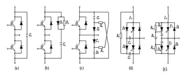
Picture 2
Figure 2 (a) is the simplest single-capacitor circuit, suitable for small-capacity IGBT modules or other devices with small capacity, but because there is no damping element in the circuit, it is easy to produce oscillation, so CS can be string into RS to suppress, this RC buffer circuit has been widely used in the protection of thyristors.
Figure 2 (b) shows that the RCD buffer circuit is used on a module consisting of two IGBTs with bridge arms. This circuit is relatively simple, but the absorption function is slightly worse than when RCD is used alone, and it is mostly used on the inverter bridge arms with small capacity components. Sometimes, two kinds of buffer circuits (a) and (b) can be used in parallel to enhance the buffer absorption function.
Figure 2 (c) is the RS cross-connected buffer circuit. When the device is turned off, CS is charged by DS to inhibit dv/dt; When the device is turned on, CS is discharged by the power supply and RS, and part of the energy is fed back to the power supply. This circuit is suitable for large-capacity devices, such as IGBT modules above 400A.
Figure 2 (d) shows the asymmetric RLCD buffer circuit on the high power GTO inverter bridge arm. In the figure, the current limiting inductor LS releases magnetic field energy through DS and RS. When GTO is turned off, CS absorbs energy through DS and feeds part of the energy back to the grid through RS, so the loss is small, and it is suitable for large-capacity GTO inverters. Among them, CS has the dual functions of absorbing electric energy and voltage clamping, and the efficiency is high.
Figure 2 (e) is a triangular absorption circuit, which is characterized by: (1) there is almost no need to connect the wires between the three capacitors, so the parasitic inductance is very small. (2) Each capacitor is involved in the work of power electronic devices, and the capacitor utilization rate is high. (3) The circuit loss is small.
The stray inductance in the lead of the buffer circuit must be limited to a minimum to prevent voltage spikes in the power electronic device when it is turned off, and to eliminate the oscillation caused by the stray inductance and CS forming a resonant loop in the buffer circuit. Therefore, R, C, D and other components in the buffer circuit should also strive to use non-inductive components.
The basic working principle of the buffer circuit is to suppress the current rise rate of the device by using the characteristics that the inductor current cannot change, and the capacitor voltage cannot change to suppress the voltage rise rate of the device. A simple buffer circuit is shown using the GTO as an example. Where L is in series with GTO to suppress the current rise rate dI/dt when GTO is on, capacitor C and diode D form a turn-off absorption circuit to suppress the terminal voltage rise rate dV/dt when GTO is off, where resistor R provides a discharge path for capacitor C. Buffer circuits come in many forms to suit different devices and different circuits.
The absorption circuit is generally composed of resistors, capacitors and diodes, often and switching tubes or diodes (including high-frequency rectifier diodes) and connected, so that the stress of the voltage on the switching tube is reduced, EMI is reduced, so that the track of the load line does not exceed the safe working area, and no secondary breakdown occurs. The flyback converter is still introduced as an example.
When the control pulse Ug shown in FIG. 1 is at low voltage t=t1, the switch tube V tends to turn off, and Ic drops. Due to the action of Lp and LLT, the collector voltage increases, forming Isnb absorbing circuit current to maintain the primary winding current Ip of the transformer unchanged (Ip=IC 10 ISNb).
If the switching tube V is turned off very quickly (best condition), the collector voltage change rate dUC/d/ is determined by the following formula:
With the switch tube V off, the linearly increased collector voltage Uce reaches 2 times the voltage of Ui at t=t3. After a short time (the delay depends on the size of the primary to secondary leakage inductance), when the secondary winding voltage rises to Ucz plus the voltage drop of D2, a circular rising current Iso is formed. At this time, the flyback current will be commutated from the primary to the secondary circuit, the rate of commutation is determined by the secondary leakage inductance and the external inductance capacitance.
Figure 1 shows the waveforms of the primary and secondary commutation processes. When t=t2 and Ip=0, 70% of the Uce=Uceo of the switch tube V is good. After that, under Isnb charging, Uce continues to rise diagonally, and when it rises to 2×Ui, the P4 voltage of the polarity reversal is coupled to △, enough to make D3 conduction, so IFB appears at t=t3, inhibiting the continued rise of Uce. At IFB=0, the secondary reaches the I's current stabilizer value.
If the above ideal situation is to be achieved, it needs to be carefully selected parameters and experimental adjustments. Figure 2 shows the absence of absorption links. Figure 3 shows the situation with the absorption link.
It is worth pointing out that if the switch tube V is equipped with a radiator, the radiator is a collector (or electrically isolated heat transfer type). When there is a capacitor between the collector of the switch tube V and the common line of the power supply, it provides an additional path for the collector current. It is also the fact that causes the collector current to exist. However, it is related to installation and cannot be confused with the Miller current effect present in the switching tube itself. In addition, its value is also relatively large, and its existence is good for reducing dUcd/dt.
The buffer circuit of power electronic devices (snubbercircuit), also known as the absorption circuit, is an important protection circuit of power electronic devices, which is not only used for the protection of semi-controlled devices, but also plays an important role in the application technology of fully controlled devices (such as GTR, GTO, power MOSFET and IGBT, etc.).
When the thyristor is turned on, in order to prevent the excessive current rise rate and burn the device, a choke inductor is often inserted in the main circuit to limit the excessive di/dt, and the series inductor and its accessories comprise the opening buffer circuit, or series buffer circuit. When the thyristor is turned off, the voltage regulator of the power supply | is suddenly applied to the pipe. In order to suppress the instantaneous overvoltage and excessive voltage rise rate, and to prevent the excessive junction capacitance current flowing inside the thyristor from accidentally triggering, a RC network needs to be connected in parallel at both ends of the thyristor to form a turn-off buffer circuit, or parallel buffer circuit.
GTR, GTO and other fully controlled self-switching devices must be equipped with on-off and off-off buffer circuits in practical use. But its function is different from the buffer circuit of thyristor, and the circuit structure is also different. The main reason is that the operating frequency of the fully controlled device is much higher than that of the thyristor, so the on-off and on-off loss is one of the important factors affecting the normal operation of the switching device. For example, GTR is prone to secondary breakdown in the dynamic switching process, which is directly related to the switching loss. Therefore, it is very important to reduce the switching loss of the fully controlled device, and the main role of the buffer circuit is exactly this, that is, GTR and power MOSFET use the buffer circuit to suppress di/dt and du/dt, mainly in order to change the switching trajectory of the device, so that the switching loss is reduced, and then the device runs reliably.
Mall Dynamic
